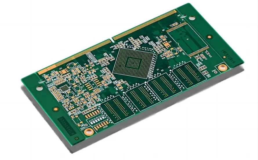
What are HDI PCBs?
High-Density Interconnect (HDI) PCBs are super cool circuit boards. They use fancy tricks to pack a ton of stuff into a tiny space. These boards stand out from regular PCBs with nifty features like microvias, blind and buried vias, thin traces, and lots of layers. The main goal is to cram in more functions without making the board bigger. This makes them perfect for sleek gadgets that need to stay small but work great.
HDI PCBs use micro-vias, which are tiny holes through just a few layers. They also use blind and buried vias to keep things compact. This lets them fit more parts and complex wiring. More layers can be added without bulking up the board. Plus, shorter traces boost signal integrity and cut down on noise or signal fuzz.

Role of HDI PCBs in Electronic Design
Gadgets today are getting smaller but doing more. They need boards that handle big jobs in tiny spaces. HDI PCBs are key players here. They squeeze in more parts and features into a small area.
In phones and wearables, HDI designs fit powerful chips, memory, sensors, and wireless bits into slim cases. Smartphones, tablets, and wearable tech all lean on HDI PCBs for their small size and zippy functions.
Smart TVs and gaming consoles use HDI PCBs for cool stuff like high-definition screens, voice controls, and internet links. In telecom gear like base stations, routers, and switches, HDI boards keep data zipping fast with little signal loss.
Cars use HDI tech in infotainment, ADAS (Advanced Driver Assistance Systems), and engine controls for trusty performance in tight spots. Medical devices, like diagnostic tools or implants, also love HDI PCBs for their small size and solid work in critical jobs. Discover Silkbridge’s HDI solutions.
Benefits of HDI PCBs
HDI PCB tech brings some awesome perks:
- Miniaturization: Packs tons of parts into a tiny space. This is huge for making sleek, powerful gadgets.
- Better Performance: Thin traces and vias make signals travel smoother, cutting noise and loss. This rocks for fast apps.
- Cost-Effective in Big Batches: Making HDI PCBs can be tricky, but they save money when made in big numbers.
- Super Reliable: Precise designs lower defect risks and handle heat better.
- Supports Cool Features: HDI PCBs work with new tech like 5G modules, IoT sensors, and AI chips, making them key for next-gen gadgets.
Challenges in HDI PCB Design
HDI tech has tons of perks, but it’s not all easy:
- Tricky Design: HDI PCBs need deep know-how of electrical stuff. Tighter spaces make placing parts tougher.
- Making Them: Building HDI PCBs uses fancy tools like laser drilling, which can cost more. Small batches are especially pricey.
- Heat Issues: With more power in small spaces, overheating is a worry. Good heat plans are needed early on.
- Testing: The packed design makes defects trickier to spot. X-ray checks and other tests are a must.
Best Practices for HDI PCB Design
To tackle challenges and get the most out of HDI PCBs:
- Smart Part Placement: Putting parts in the right spots cuts trace length. This lowers interference and makes wiring smooth.
- Fancy Design Tools: Cool software helps handle multi-layer wiring and keeps signals clear.
- Heat and Power Plans: With lots of parts, heat control is key. Thermal vias or copper planes help spread heat.
- Team Up with Makers: Working closely with PCB builders ensures the design works without losing quality.
HDI PCB Turnkey Services from Silkbridge

Silkbridge offers full-on solutions for advanced electronics needing high-density interconnects PCB. They handle everything from design to mass production.
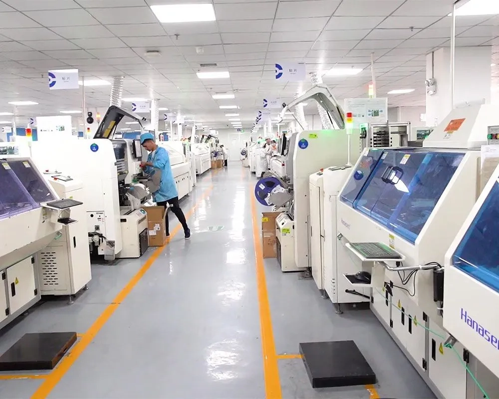
Their R&D team uses simulation software to make optimized layouts. Prototypes get tested before going big. Silkbridge uses 12 fully automated Surface Mount Technology (SMT) lines with optical inspection systems (AOIs), solder paste checks (SPI), and auto pick-and-place machines for spot-on assembly at scale.
Quality is locked in at every step. Each SMT line is automated for steady results. After assembly, environmental tests ensure PCBs handle tough conditions.
Silkbridge also does complete product assembly. Their lines churn out tons of finished products monthly in controlled settings.
For clients wanting start-to-finish services—from idea to shipping—Silkbridge brings top value, covering product builds with plastic, metal, and electronics all in-house.
- WhatsApp: +86 18122838771
- Phone: +86 18122838771
- Email:contact@silkbridgeltd.com
FAQ
Q1: What industries benefit most from using HDI PCBs?
Mobile devices, consumer electronics, telecom, cars, and medical gear lean on HDI tech for small, powerful designs.
Q2: Are HDI PCBs more expensive than traditional ones?
They can cost more upfront due to tricky making processes. But big batches save money by using space and parts better.
Q3: What makes Silkbridge a reliable partner for producing HDI boards?
Silkbridge offers a full package—award-winning R&D, auto SMT lines, strict quality checks, and final assembly. Their know-how across industries ensures top-notch delivery.
Q4: How does Silkbridge ensure quality during mass production?
Each SMT line has optical inspection systems. Post-assembly environmental tests and final checks match client specs before shipping.


