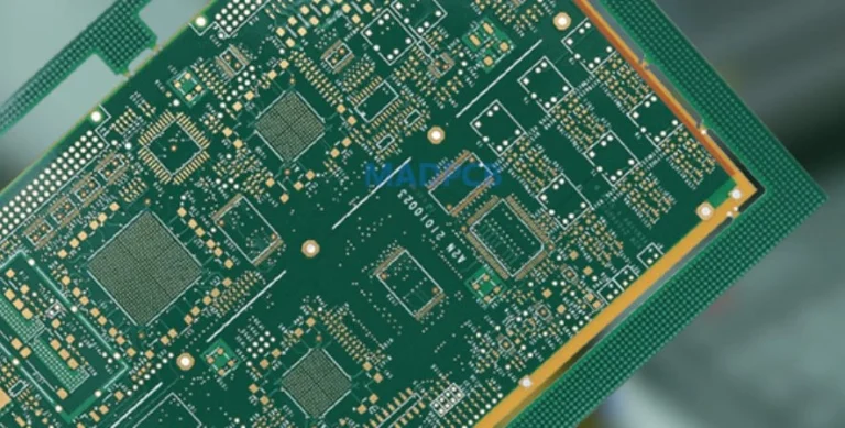
What Is HDI PCB and Why Is It Important?
HDI PCBs stand out due to their tight wiring setup in a small space. They use tiny holes called microvias, hidden or buried vias, and a step-by-step layering method to boost performance while keeping things small. This setup helps engineers create tinier, quicker, and more powerful electronic gadgets.
These boards bring cool benefits like speedy signal flow, better protection against electronic noise (EMC), less power use, and a lighter, smaller build. Thanks to these strengths, HDI PCBs are a top pick in fields where size matters and power is key—think smartphones, car systems, airplane tools, and medical gear.
 PCB Design: Best Practices for Complex Products插图")
Challenges in HDI PCB Design
Even with their perks, HDI PCBs come with tough hurdles that need special know-how and equipment. Some common issues are: Tight space for wiring paths—dense setups leave little room to work. Signal problems—fast signals can weaken if things don’t match up right. Making troubles—creating microvias and layering steps needs strict control. Higher cost—fancy materials and steps make HDI boards pricier.
This is why teaming up with a skilled PCB design service is so important. Trusted experts help tackle these issues while making sure the design meets both power needs and production rules.
Best Practices for HDI PCB Design
To get the best results and steady performance from high-density interconnect (HDI) PCB designs, engineers should stick to tried-and-true tips. These cover planning layers, via choices, signal care, heat control, and ease of making.
Strategic Layer Stack-Up Planning
Good layer planning is the base of any HDI board. For top outcomes:
- Keep layer stacks even to avoid bending.
- Switch between signal and ground or power layers for steady control.
- Place fast signals near guide layers.
Working with seasoned PCB designers early on helps pick the right layer count, materials, thicknesses, and via setups for the project.
Microvia and Via-in-Pad Techniques
Microvias are a must for tight designs without losing power. Go for laser drilling to stay precise and dependable. Keep microvia ratios under 1:1. Think about stacking or spacing microvias based on wiring needs.
For small parts like BGAs (Ball Grid Arrays), via-in-pad setups save space. Make sure vias are filled and coated well to dodge soldering snags.
Impedance Control and Signal Integrity
Fast signals in packed designs need strict control to avoid issues. Use guided traces with the right size and gaps. Skip sharp 90-degree turns to cut down on bounce-back. Stick to paired routing for speedy signals.
Teaming up with a savvy PCB hardware design expert ensures deep checks before and after layout for signal strength.
 PCB Design: Best Practices for Complex Products插图1")
Thermal Management
As gadgets get smaller but do more, handling heat turns into a big worry.
- Add thermal vias to pull heat away from hot spots.
- Pick materials that handle high heat and don’t expand much.
- Spread power and ground layers evenly to keep heat low.
Smart heat planning is key for lasting board trust—especially in high-stakes uses like airplane or car tech.
DFM (Design for Manufacturability)
Making HDI boards involves tricky steps like layered building and laser drilling. To keep costs down and avoid delays:
- Stick to the maker’s smallest trace width and spacing rules.
- Cut down on layering rounds.
- Use common pad sizes for easy building.
A sharp PCB design engineer weaves DFM tips into the layout from the get-go—making sure your product works and can be built smoothly.
CAD Tools and Simulation
Today’s EDA tools are a game-changer for designing HDI PCBs. Programs like Altium Designer, Cadence Allegro, or Mentor Graphics give you:
Hidden or buried via setups; Easy routing for packed BGAs; Tools for impedance and layer planning.
Strong simulation options spot risks like EMI (electromagnetic interference), signal overlap, or power flaws early on—saving you from pricey fixes down the road.
Importance of Working with an Expert PCB Design Partner
HDI projects need skills across electric, physical, and heat areas. A full-service team should bring:
Design advice; Signal and power checks; Early builds and tests; Support for big batches.
That’s why many businesses pick all-in-one PCB design partners with wide skills, cutting hassle while speeding up launch time.
Future Trends in HDI Technology
Looking ahead, HDI PCBs will get even smaller lines, more layers, built-in parts, bendy bases, and links to new tech like 5G or AI chips. Fresh ideas like 3D printing methods or cutting-edge materials will open doors—think super-slim wearables or IoT gadgets with amazing tricks.
Let’s Conclude
By sticking to top tips—from layer setup to DFM—and using modern tools with expert help, firms can handle the tough parts of high-density interconnect (HDI) PCB work. This way ensures solid results while keeping costs smart across fields from everyday gadgets to airplane systems.
FAQ
Q1: What makes an HDI PCB different from standard PCBs?
A1: HDI PCBs have microvias, hidden or buried vias, more layers, and thinner lines than regular PCBs—fitting more stuff in a tiny spot.
Q2: Why is impedance control critical in HDI designs?
A2: Fast signals can bounce or twist if impedance isn’t tight—hurting how the whole system runs.
Q3: Can I use standard CAD software for HDI design?
A3: You’ll need special EDA tools that handle stuff like laser-drilled vias or BGA routing—for spot-on checks before making.
Q4: How do I ensure my HDI board is manufacturable?
A4: Team up with your maker from day one; follow DFM rules on trace sizes and gaps; keep layering steps low; use normal pad sizes.
Q5: What industries benefit most from HDI technology?
A5: Everyday tech (smartphones), car setups (ADAS), airplane control units, medical tools—all depend on small, strong boards made with HDI tech.
Why Choose Silkbridge for HDI PCB Design and Production and Assembly?
At Silkbridge, we’re proud to blend British creativity with Chinese making know-how. Started by a British engineer in 2014 in Guangdong Province, our firm has grown into a top name for high-quality production worldwide.
Our power comes from our prize-winning R&D crew and our all-in-one skills—from idea stage to final build. We cover everything: product ideas, plastic, metal, electronics, and putting the final piece together—all under one roof.
For folks needing exact electronics, Silkbridge runs fully auto PCB SMT (Surface Mount Technology) lines with top-notch gear from big global names, ensuring steady quality for small tests or big runs.
With ISO 9001 stamps for plastic and electronic making, quality is locked into every step—from first checks to AOI/X-ray scans.
We also make shipping easy: we handle full delivery options like DDP shipping, so customs or import fees aren’t your headache.
Whether you’re crafting next-wave personal gadgets or vital industry tools, Silkbridge gives a one-stop service that keeps even the trickiest production jobs as simple as can be for our clients. Get in touch with us now on our business WhatsApp at https://wa.me/8618122838771 or call +86 8618122838771.