Printed circuit boards are an essential ingredient but among the most invisible parts in the electronics world. From powering your smartphones to making those giant industrial machinery function, it is the heart of nearly all advanced electronic gadgets. For the company or individual who wants to understand something about PCB design and the technical terms applied, they need to know something very important: the terminology. This guide gives a comprehensive overview of PCB design, terminology, and major steps in the design process, with the needs of B2B audiences in need of reliable PCB design services in mind.
What Exactly Is a PCB?
A Printed Circuit Board is a support for electronic circuits. Essentially, it is a flat board, normally of fiberglass or other non-conductive materials, having conductive pathways etched or printed on its surface. These pathways, called traces, serve like wires to carry the electrical signals between different components mounted on the board, such as resistors, capacitors, and integrated circuits.
Unlike traditional point-to-point wiring, PCBs offer several advantages:
- Reliability: With PCBs, the risk of loose connections and short circuits is minimized, making electronic devices more reliable.
- Compactness: PCBs facilitate the dense packing of components, allowing for smaller and more portable devices.
- Cost-effectiveness: Automated processes allow PCBs to be mass-produced at a lower cost, making them an economical solution for manufacturers.
Types of PCBs
They are available in numerous variants for specific uses. Knowledge about these variants is thus very crucial for the company to make an informed decision about the optimum PCB solution for its product.
Single-Sided PCBs: The least complicated of the PCBs, they are those that carry conductive material on one side only. They generally find deployment in applications that have low costs, such as simple consumer electronics and household appliances.
Double-Sided PCBs: In a double-sided PCB, both sides are coated with conductive material. This allows the mounting of more complicated circuits. Double-sided PCBs find wider applications in more sophisticated uses such as power supplies and communications equipment.
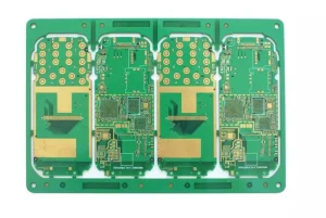
Multi-Layer PCBs: These consist of multiple layers of conductive material separated by insulating layers. They find their use in high-performance applications such as smartphones, computers, and medical devices. They are used where space is limited but component density is very high.
How to Design a PCB
Designing a PCB is a well-structured process that requires equally specialized knowledge and tools. A good PCB design guarantees the functionality and performance of the device. Below are the important steps that outline the design process for a PCB:
Step 1: Schematic Design
Schematic Diagram: The symbolic representation of the electrical connections between components is the first stage in designing a PCB. At this stage, only the electrical relationships, not the physical placement of parts, are taken into consideration. The schematic diagram forms the blueprint for the successive stages of design.
Step 2: PCB Layout
The completed schematic then advances the designer into the stage of the layout of the PCB. It is the stage involving the physical component placement and tracing of routes or traces. Special CAD software has to be used, which lays out optimally to meet the schematic design rules and constraints. The major tasks or operations performed in the layout are as follows:
- Component Placement: Strategic placement of components ensures the board functions as intended and minimizes signal interference.
- Routing: The traces are drawn to connect the components, requiring careful attention to signal integrity, power distribution, and noise reduction.
- Plane Creation: For multi-layer boards, planes of copper are created on inner layers to provide power and ground connections.
Step 3: Design Rule Check
Once the layout is complete, a design rule check is performed, commonly called a DRC. This is an automated check of the design against pre-defined constraints such as minimum trace widths, spacing and hole sizes. The DRC prevents a number of possible errors that may affect functionality or manufacturability.
Step 4: Gerber File Generation
Finally, Gerber files are generated. These are the industry standard files which contain all the information needed for the fabrication of the PCBs. The Gerber file is given to the PCB manufacturer who will manufacture the actual board.
Key PCB Terminology
The world of PCB design has its own sets of terms. Knowing these terms is important to making sense out of the design process:
- Trace: The conductive path on a PCB, which functions like a wire.
- Pad: The copper area where components are soldered onto the PCB.
- Via: A hole that connects traces on different layers of the PCB.
- Solder Mask: A protective layer that prevents solder bridges between traces and protects the board from environmental damage.
- Silkscreen: A layer of ink that labels the components and provides other markings.
- Through-Hole Components: Components with leads that go through the PCB and are soldered on the opposite side.
- Surface-Mount Devices (SMDs): Components that are mounted directly onto the PCB’s surface.
- BGA (Ball Grid Array): A type of SMD with solder balls beneath it, commonly used for high-density connections.
Advanced Considerations in PCB Design
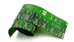
High-Density Interconnect and Rigid-Flex PCBs are among the other key terminologies targeted toward more advanced solutions of PCBs. HDI PCBs realize higher performance through the use of microvias and fine-pitch components targeted toward compact, high-performance devices in smartphones and medical equipment. Conversely, Rigid-Flex combines the strength of rigid boards with the flexibility of flexible circuits; such is expected to find application in aerospace and automotive industries due to reasons such as saving space and reducing weight.
Silkbridge: Your Partner in PCB Design & Manufacturing
For the enterprise seeking high quality, dependability, and affordable PCB solutions, the leader is Silkbridge Electronic Technology. With an immense range of services on offer, Silkbridge can deliver to meet all needs for either standard or high-performance PCB design. Here’s how Silkbridge can support your business:
Comprehensive PCB Design Services: Silkbridge designs single-layer, double-layer, and multi-layer PCBs for industries ranging from consumer electronics to medical devices. The designs are optimized for specific customer needs to realize the best possible performance and manufacturability of the product.
Flexible and Rigid-Flex PCB: Silkbridge has specialized in flexible PCBs that find their applications in very space-constrained environments, while the rigid-flex PCBs are highly durable, perfect for dynamic applications in automotive and aerospace sectors.
HDI PCB Solutions: Silkbridge has rich experience in HDI PCB design for industries that require high-density interconnections, miniaturized designs, and advanced functionalities in devices. This includes but is not limited to smartphones, wearables, and IoT devices.
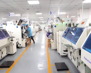
Advanced Manufacturing Capabilities: SMT-A, Automated Optical Inspection-AOI, and X-ray Inspection form the cornerstone of superior standards from manufacturing processes adopted at Silkbridge; hence leading quality standard mechanisms. There was also the system for validating design through several simulated tests with thorough follow-through of various assembly test levels.
Global Reach and Expertise: Silkbridge provides service to customers in virtually every market: the USA, Western Europe, and Japan. It is also established in various industries such as automotive, medical devices, and consumer electronics. Its products have appeared in major retail chains such as Walmart and Costco and online on Amazon:
It can give necessary support with expertise, whether one needs standard PCBs, flexible PCBs, or advanced HDI designs. Silkbridge is committed to quality, innovation, and customers, earning them the confidence of businesses all over the world.
Why Choose Silkbridge?
Silkbridge provides a one-stop solution for your PCB design and manufacturing needs. Their experience in the provision of PCB design services is backed by years of experience and dedication to delivering top-notch, reliable products. With the focus on DFM and adherence to industry standards, Silkbridge ensures your PCB designs are ready for high-volume production with minimal risk of errors. It also involves the designing and manufacturing of goods relating to simple consumer electronics projects or complex and more advanced medical devices for which Silkbridge is very well prepared.
A business in need of a reliable supplier of PCBs finds at Silkbridge the right mix of state-of-the-art technology, quality assurance, and customer-oriented services. For more about how their PCB design and manufacturing services can help take your product development to the next level, contact Silkbridge today.


