Printed circuit boards form the backbone of nearly each electronic device, providing both connective and supportive elements through which components like smartphones, laptops, medical devices, and industrial equipment can function just as they were intended. PCBs help direct the flow of electrical signals energizing our increasingly interconnected world-and, quite frankly, make them pretty fundamental in terms of modern electronics manufacturing.
What is a PCB?
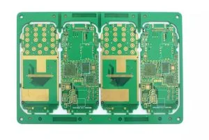
A typical printed circuit board normally includes a flat, rigid board made of some non-conducting material, usually fiberglass. The board contains conductive pathways, or traces, fabricated using copper to connect resistors, capacitors, transistors, and ICs that make up an electronic device. These conductive pathways provide a path with which electrical signals flow to and from the various parts, hence the functionality aspect of the device.
They are available in several forms: single layer, double layer, and multilayer boards depending on the complexity and performance required. Inventions have also taken place in the material used for the PCBs, such as flexible PCBs and rigid-flex PCBs for specific applications.
PCB Manufacturing Process: A Step-by-Step Journey
Fabrication of the PCB involves an elaborative process with various stages, as the conceptual design is made to become an electronic component. Now, each stage for the fabrication process of the PCB will be elaborated:
1. Design and Output:
It all starts with a detailed design, for which circuit designers use special CAD software. The latter carries all the details concerning component placement, conductive pathway routing, and other specifications. The same is then exported in a readable format for equipment that will manufacture the PCBs, normally in Gerber file format, and guides the production process.
The research firm TechNavio projects that between 2021 and 2025, the global market for the design of PCB will be developing at a growth rate of 7% annually. It is predicted based on increased demand observed within three key sectors driving this growth: consumer electronics, automotive, and telecommunications. Growth in this regard carries directly into the importance of precision within modern electronics design.
2. Imaging and Photoresist Application:
The photoresist material on the copper-clad laminate board receives the PCB design. Where this photoresist material has been exposed to light, it becomes hard; in places where it did not get the light, it remains soft and can be washed away. This will leave a pattern of exposed copper that provides the required paths of conduction.
3. Etching:
During etching, a PCB is subjected to some kind of chemical solution that peels away the unprotected copper until the desired traces remain. In fact, etching is one more critical process because everything should be very thoroughly monitored since defects here-like copper slivers and patches of unetched areas-are detrimental to further high-quality performance.
4. Drilling:
Precision drilling machines manufacture vias (holes) in a board, which are required to connect the layers on multilayer PCBs and through-hole components. Computer-aided programming enables this process to be done at very high levels of automation; some manufacturers even use laser techniques for finer detail while drilling.
5. Layer Bonding (for Multilayer PCBs):
In case of a multilayer PCB, several layers of copper and insulating materials are bonded with each other through heat and pressure in the lamination process. Normally, multilayer PCBs are applied in high-performance applications that also include smartphones and medical devices, where the complexity and compact design play a crucial role.
6. Solder Mask Application:
A solder mask is applied that prevents the copper traces from oxidation and avoids solder bridges during the assembly of components. The solder mask is usually green but can be made in different colors for aesthetic purposes or for brand differentiation.
7. Silkscreen Printing:
Labels and markings are made on the PCB by a process called silkscreen printing. These make the assembling of the board easier and allow a technician to easily find various components and connections whenever some fault needs to be tracked. Such markings also assist in meeting industrial standards and regulations.
8. Surface Finishing:
This stage treats the exposed areas of copper to enhance solderability and prevent corrosion. Standard finishes include hot air solder leveling, immersion gold, and electroless nickel immersion gold.
9. Testing:
The several test techniques involved are in-circuit testing, flying probe testing, and functional testing just to ensure that the quality of the PCB is in order. Testing is a very necessary aspect in which it has to be ensured that the end product will work perfectly without any defect that would eventually lead to device failures.
10. Profiling and V-Scoring:
The individual boards are then routed or V-scored to separate them from the panel in preparation for the assembly process.
PCB Assembly Process
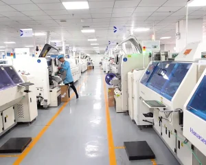
The next step in this process involves assembling the fabricated PCB with the electronic components. This basically consists of the following operations:
Solder Paste Application: The solder paste is applied on the pads where the components are supposed to sit.
Component Placement: Stenciling places the SMDs onto the board, which are then automatically mounted by pick-and-place machines.
Reflow Soldering: The PCB passes through a reflow oven where the solder paste is melted to form reliable electrical connections between the components and the board.
Through-Hole Component Insertion: Components to be inserted with leads through the PCB are either inserted manually or by automated tools.
Wave Soldering:This process utilizes a wave of molten solder for attaching through-hole components to the board.
Inspection and Testing: The assembled board undergoes inspection using automated optical inspection (AOI) and X-ray inspection to ensure high-quality connections.
The Importance of Precision and Quality Control
Precision is key during the manufacturing process of PCBs. Minor mistakes in trace widths, hole sizes, or component placements may easily cause device malfunction. For instance, the National Institute of Standards and Technology (NIST) has set that as small as 0.1mm deviations in trace widths may affect the performance of a PCB, especially for high-speed digital circuits.
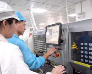
The manufacturers also employ state-of-the-art equipment for the purpose of automated optical inspection-AOI and X-ray inspection for value addition at various levels. Such technologies have grown so pivotal in defect recognition for the purpose of PCB assembly to be able to boast of best functional and reliable product which comes out.
Silkbridge: Your Partner in PCB Excellence
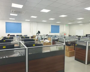
Silkbridge is a major China-based PCB manufacturer, providing one-stop services for various customer needs. The use of the latest technology along with severe quality control enables it to provide superior-quality PCBs. With a trustworthy background, it has developed trust in its global customer base regarding the supply of good-quality PCBs for different industries such as consumer electronics, automotive, telecommunications, and medical.
Why choose Silkbridge for PCB manufacturing?
In-house R&D Expertise: Award-winning R&D department that converts concepts into functional designs in close interaction with the client.
Advanced Manufacturing Capabilities: Highly automated surface-mount technology lines under the Silkbridge banner give volume and small batches depending on the size of the project.
Stringent Quality Control: Every PCB is assured through AOI and X-ray inspection to meet the highest parameters of performance and durability at Silkbridge.
Global Reach: Silkbridge serves a wide variety of international customers with timely delivery and quality service.
With proficiency in the manufacture of PCBs and assurance of quality, Silkbridge will be an ideal partner to help both startups and well-established companies bring new and innovative electronic products to the market.
Conclusion
In the manufacturing process for a PCB, there is a great deal of difference between ancient and modern electronic productions. Since modern electronic gadgets are complex, they also make sure that the reliability and high quality within them is unparalleled, and it is ultimately demanding from the PCBs. Only such products can a business get by relying on a trusted PCB manufacturer like Silkbridge.
For any further help and assistance in the manufacturing of PCBs and upgrading your electronic products to a whole new level, always feel free to get in touch with us today at Silkbridge on whatsapp https://wa.me/8618122838771 or call directly our specialist on +86 18122838771


